ChipApex | Global Electronic Components Supplier
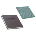
10AX016E3F27E1SG
Search Product
Search Post
— IC芯片 | 连接器 | 传感器 | 被动器件 —
Search productSearch post
— IC芯片 | 连接器 | 传感器 | 被动器件 —
Consult the customer manager about the wholesale price.
consultation hotline:86-132-6715-2157
email:chipapexlimited@gmail.com
Contact the product manager for consultation. One-stop consultation is available.
Do you want a lower wholesale price? Please send us your inquiry and we will reply immediately.


Altera 10AX016E3F27E1SG is used in FPGAs (Field Programmable Gate Array) category where interface timing, endurance expectations, and power behavior affect reliability. Key specs include Description (IC FPGA 240 I/O 672FBGA), Temperature (0°C ~ 100°C (TJ)), Package/case (672-BBGA, FCBGA), Mounting (Surface Mount), and Packaging (Tray).
What details help you quote 10AX016E3F27E1SG quickly?
Send the part number (10AX016E3F27E1SG), quantity, target delivery date, and any required packaging or documentation.
Can you confirm the operating temperature range for 10AX016E3F27E1SG?
0°C ~ 100°C (TJ)
Which Total RAM Bits is specified for 10AX016E3F27E1SG?
10086400
What is the package/case of 10AX016E3F27E1SG?
672-BBGA, FCBGA
When sourcing Altera 10AX016E3F27E1SG for FPGAs (Field Programmable Gate Array), engineers typically focus on de-risking integration and keeping validation repeatable. Designers typically use them to bridge voltage domains, protect I/O, and keep edges and thresholds well-behaved on shared buses. Across many systems, careful use of interface logic reduces integration risk by making timing and signal integrity easier to validate. In telecom and networking hardware, buffering and translation maintain timing margin on dense backplanes. Across control and timing paths, simple gating enforces sequencing and interlocks where deterministic hardware behavior is preferred over firmware. In signal conditioning, gates and inverters clean up enables, chip-selects, and edge routing when fan-out and loading would otherwise distort thresholds. In many programs, a focused validation plan surfaces the real risks earlier than additional schematic iteration. In practice, when margins are explicit and measurable, stability tends to hold up better across real deployments.
 10AX016E3F27E1SG
The activity of extra discounts on wholesale prices is in full swing…
Please fill in your contact information and we will send you the latest wholesale price list.