ChipApex | Global Electronic Components Supplier
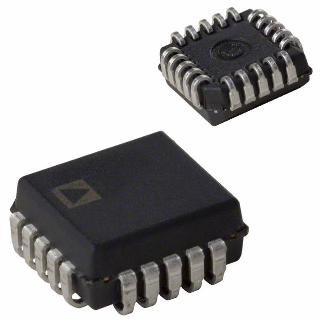
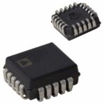
AD652JPZ
Search Product
Search Post
— IC芯片 | 连接器 | 传感器 | 被动器件 —
Search productSearch post
— IC芯片 | 连接器 | 传感器 | 被动器件 —
Consult the customer manager about the wholesale price.
consultation hotline:86-132-6715-2157
email:chipapexlimited@gmail.com
Contact the product manager for consultation. One-stop consultation is available.
Do you want a lower wholesale price? Please send us your inquiry and we will reply immediately.
Analog Devices Inc. AD652JPZ is selected in V/F and F/V Converters category when protection behavior and transient response must be validated under realistic load steps. Key specs include Description (IC V/F CONV 2MHZ 20PLCC), Package/case (20-LCC (J-Lead)), Mounting (Surface Mount), and Packaging (Tube).
What details help you quote AD652JPZ quickly?
Share the part number (AD652JPZ), quantity, target delivery date, and any packaging or documentation requirements.
What is the Supplier Device Package of AD652JPZ?
20-PLCC (9x9)
Which packaging option is listed for AD652JPZ?
Tube
Can you confirm the mounting type for AD652JPZ?
Surface Mount
Selecting Analog Devices Inc. AD652JPZ for V/F and F/V Converters usually comes down to meeting the system constraints that matter most: limits, interfaces, and testability in the real build. Engineers often validate interface conditioning and noise coupling because edge integrity and threshold behavior can dominate accuracy. End-to-end behavior depends on references, layout, filtering, and the real impedance environment, so verification is done on the assembled PCB. Teams typically validate noise and settling on the actual PCB stack-up because parasitics and coupling often dominate datasheet-to-board gaps. Across energy metering, accuracy is maintained across noisy mains and wide temperature swings. Within isolated measurement systems, frequency signaling reduces gain error from cable resistance and ground shifts compared to low-level voltage transmission. In real deployments, a small set of stress tests often identifies the limiting assumptions long before production ramp.
 AD652JPZ
The activity of extra discounts on wholesale prices is in full swing…
Please fill in your contact information and we will send you the latest wholesale price list.