ChipApex | Global Electronic Components Supplier
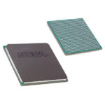
10AX022E3F27E1SG
Search Product
Search Post
— IC芯片 | 连接器 | 传感器 | 被动器件 —
Search productSearch post
— IC芯片 | 连接器 | 传感器 | 被动器件 —
Consult the customer manager about the wholesale price.
consultation hotline:86-132-6715-2157
email:chipapexlimited@gmail.com
Contact the product manager for consultation. One-stop consultation is available.
Do you want a lower wholesale price? Please send us your inquiry and we will reply immediately.
Altera 10AX022E3F27E1SG is used in FPGAs (Field Programmable Gate Array) category where interface timing, endurance expectations, and power behavior affect reliability. Key specs include Description (IC FPGA 240 I/O 672FBGA), Temperature (0°C ~ 100°C (TJ)), Package/case (672-BBGA, FCBGA), Mounting (Surface Mount), and Packaging (Tray).
Any tips for reliable operation with 10AX022E3F27E1SG?
Ensure robust power sequencing, adequate decoupling capacitors, and verify signal integrity on high-speed data buses.
Which Supplier Device Package is listed for 10AX022E3F27E1SG?
672-FBGA (27x27)
How is 10AX022E3F27E1SG mounted?
Surface Mount
What supply voltage range does 10AX022E3F27E1SG require?
0.87V ~ 0.93V
In real deployments, across many FPGAs (Field Programmable Gate Array) builds, Altera 10AX022E3F27E1SG is reviewed for predictable behavior, supportability, and stable qualification evidence. Across mixed-voltage boards, clean translation and buffering reduce contention risk and protect interfaces during hot-plug and brownout events. They implement deterministic digital interface and control functions such as buffering, decoding, timing, and level translation with predictable latency. Across aerospace electronics, predictable propagation and stable thresholds support qualification evidence. In signal conditioning, gates and inverters clean up enables, chip-selects, and edge routing when fan-out and loading would otherwise distort thresholds. In high-speed boards, small logic functions support reset distribution and clock-domain controls where skew and ringing must be managed.
 10AX022E3F27E1SG
The activity of extra discounts on wholesale prices is in full swing…
Please fill in your contact information and we will send you the latest wholesale price list.