ChipApex | Global Electronic Components Supplier
10AX022E3F27I1SG
Search Product
Search Post
— IC芯片 | 连接器 | 传感器 | 被动器件 —
Search productSearch post
— IC芯片 | 连接器 | 传感器 | 被动器件 —
Consult the customer manager about the wholesale price.
consultation hotline:86-132-6715-2157
email:chipapexlimited@gmail.com
Contact the product manager for consultation. One-stop consultation is available.
Do you want a lower wholesale price? Please send us your inquiry and we will reply immediately.


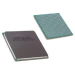
Altera 10AX022E3F27I1SG is selected in FPGAs (Field Programmable Gate Array) category when storage behavior must remain predictable across temperature and production variance. Key specs include Description (IC FPGA 240 I/O 672FBGA), Temperature (-40°C ~ 100°C (TJ)), Package/case (672-BBGA, FCBGA), Mounting (Surface Mount), and Packaging (Tray).
Which Number of Logic Elements/Cells is listed for 10AX022E3F27I1SG?
220000
Which package/case is listed for 10AX022E3F27I1SG?
672-BBGA, FCBGA
Which Total RAM Bits is specified for 10AX022E3F27I1SG?
13752320
How is 10AX022E3F27I1SG packaged?
Tray
Altera 10AX022E3F27I1SG shows up under FPGAs (Field Programmable Gate Array) when designers want a well-bounded, datasheet-driven building block instead of a fragile board-level workaround. They are generally valuable when interface compatibility and hardware timing must be guaranteed rather than "best effort". They are typically used when timing closure and interface robustness need to be provable on the bench and repeatable in production. In industrial automation, deterministic logic supports interlocks and fault handling near EMI sources. Across signal conditioning, gates and inverters clean up enables, chip-selects, and edge routing when fan-out and loading would otherwise distort thresholds. In high-speed boards, small logic functions support reset distribution and clock-domain controls where skew and ringing must be managed. In practice, within test fixtures, gating simplifies stimulus routing so measurement steps remain repeatable across cycles and operators.
 10AX022E3F27I1SG
The activity of extra discounts on wholesale prices is in full swing…
Please fill in your contact information and we will send you the latest wholesale price list.