ChipApex | Global Electronic Components Supplier
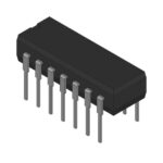
4011BDM
Search Product
Search Post
— IC芯片 | 连接器 | 传感器 | 被动器件 —
Search productSearch post
— IC芯片 | 连接器 | 传感器 | 被动器件 —
Consult the customer manager about the wholesale price.
consultation hotline:86-132-6715-2157
email:chipapexlimited@gmail.com
Contact the product manager for consultation. One-stop consultation is available.
Do you want a lower wholesale price? Please send us your inquiry and we will reply immediately.
National Semiconductor 4011BDM is used in Gates and Inverters category where integration and verification need to stay predictable. Key specs include Description (IC GATE NAND 4CH 2-INP 14CDIP), Series (4011B), Packaging (Bulk), Package/case (14-CDIP (0.300", 7.62mm)), and Mounting (Through Hole).
How do I confirm compatibility for 4011BDM?
Match mechanical footprint first, then verify electrical limits and operating conditions against your system constraints.
Which Number of Circuits is specified for 4011BDM?
4
What current consumption is specified for 4011BDM?
30 µA
How is 4011BDM packaged?
Bulk
National Semiconductor 4011BDM in the Gates and Inverters category is typically selected when engineers need predictable, spec-driven behavior in a production design. In mixed-voltage boards, clean translation and buffering reduce contention risk and protect interfaces during hot-plug and brownout events. They implement deterministic digital interface and control functions such as buffering, decoding, timing, and level translation with predictable latency. Across telecom and networking hardware, buffering and translation maintain timing margin on dense backplanes. Within high-speed boards, small logic functions support reset distribution and clock-domain controls where skew and ringing must be managed. In test fixtures, gating simplifies stimulus routing so measurement steps remain repeatable across cycles and operators. With interfaces and limits agreed, the next step is proving measured behavior on the real PCB and harness. The payoff is a design that is easier to qualify, easier to service, and more stable across environments.
 4011BDM
The activity of extra discounts on wholesale prices is in full swing…
Please fill in your contact information and we will send you the latest wholesale price list.