ChipApex | Global Electronic Components Supplier
AD650SD/883B
Search Product
Search Post
— IC芯片 | 连接器 | 传感器 | 被动器件 —
Search productSearch post
— IC芯片 | 连接器 | 传感器 | 被动器件 —
Consult the customer manager about the wholesale price.
consultation hotline:86-132-6715-2157
email:chipapexlimited@gmail.com
Contact the product manager for consultation. One-stop consultation is available.
Do you want a lower wholesale price? Please send us your inquiry and we will reply immediately.
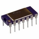
Analog Devices Inc. AD650SD-883B is selected in V/F and F/V Converters category when protection behavior and transient response must be validated under realistic load steps. Key specs include Description (IC F/V & V/F CONV 1MHZ 14CDIP), Package/case (14-CDIP (0.300", 7.62mm)), Mounting (Through Hole), and Packaging (Tube).
Any tips for derating and validation for AD650SD-883B?
Validate at worst-case temperature and load, confirm thermal headroom, and check protection and startup behavior with margin.
Which Qualification is specified for AD650SD-883B?
MIL-STD-883
What mounting type does AD650SD-883B use?
Through Hole
What packaging is listed for AD650SD-883B?
Tube
When sourcing Analog Devices Inc. AD650SD-883B for V/F and F/V Converters, engineers typically focus on de-risking integration and keeping validation repeatable. In real deployments, they often include analog front-end functions such as filtering, buffering, multiplexing, or isolation that reduce external component count. Engineers typically pay close attention to grounding, references, interface timing, and loading so end-to-end performance is preserved on the PCB. Engineers often validate interface conditioning and noise coupling because edge integrity and threshold behavior can dominate accuracy. Across industrial automation, signal-chain choices are validated for EMI resilience and repeatable accuracy near motors and contactors. In isolated measurement systems, frequency signaling reduces gain error from cable resistance and ground shifts compared to low-level voltage transmission. Within retrofits, V/F and F/V blocks help interface legacy analog sensors with modern digital counters and controllers.
 AD650SD/883B
The activity of extra discounts on wholesale prices is in full swing…
Please fill in your contact information and we will send you the latest wholesale price list.