ChipApex | Global Electronic Components Supplier
SEARCH
Search Product
Search Post
— IC芯片 | 连接器 | 传感器 | 被动器件 —
Search productSearch post
— IC芯片 | 连接器 | 传感器 | 被动器件 —
The trend of science and technology is changing rapidly.
Field-Programmable Gate Arrays (FPGAs) represent a revolutionary leap in digital circuit design, offering unparalleled flexibility and performance. Unlike traditional Application-Specific Integrated Circuits (ASICs), which are hardwired for a single function, FPGAs can be reprogrammed to perform a wide range of tasks, making them ideal for prototyping, rapid development, and applications requiring frequent updates.
At the heart of an FPGA lies its unique architecture, which consists of three primary components: Configurable Logic Blocks (CLBs), Interconnect Resources, and Input/Output (I/O) Blocks.
CLBs are the fundamental building blocks of an FPGA, responsible for executing logical operations. Each CLB typically contains a Lookup Table (LUT), multiplexers, and flip-flops. The LUT, a small memory unit, stores the truth table of a logical function, enabling it to implement any combination of inputs and outputs. By configuring the LUT, designers can define the logical behavior of the CLB, such as AND, OR, XOR, or more complex functions.
Flip-flops within the CLB provide sequential logic capabilities, allowing the FPGA to store and manipulate data over time. This combination of combinatorial and sequential logic enables FPGAs to handle a wide variety of tasks, from simple data processing to complex state machines.
Interconnect resources are the “wires” that connect the CLBs and I/O blocks, forming the internal routing network of the FPGA. These resources include various lengths of interconnect lines and programmable switches, which determine how signals are routed between different parts of the chip. The flexibility of the interconnect network allows designers to optimize the layout of their circuits, minimizing signal delays and improving overall performance.
The interconnect architecture is hierarchical, with local, intermediate, and global interconnects. Local interconnects provide short-distance connections between adjacent CLBs, while intermediate and global interconnects facilitate longer-distance communication across the chip. This hierarchical design ensures efficient signal routing and reduces congestion in high-density designs.
I/O blocks serve as the interface between the FPGA and the external world. They support a wide range of voltage levels and communication protocols, enabling the FPGA to interact with various devices, such as sensors, actuators, and other integrated circuits. Each I/O block typically includes input and output buffers, level shifters, and protection circuitry to ensure reliable signal transmission and compatibility with different standards.
The programmability of I/O blocks allows designers to configure them for specific applications, such as high-speed serial communication, parallel data transfer, or general-purpose I/O. This flexibility makes FPGAs suitable for a diverse range of industries, from telecommunications to automotive electronics.
The ability to reprogram an FPGA is one of its most powerful features. FPGAs are programmed using Hardware Description Languages (HDLs), such as Verilog or VHDL, which allow designers to describe the behavior of their circuits at a high level of abstraction. These HDL descriptions are then synthesized into a netlist, a low-level representation of the circuit that specifies the connections between the CLBs and other resources.
Once the netlist is generated, it undergoes placement and routing, a process that maps the netlist onto the physical resources of the FPGA. Placement determines the location of each CLB and I/O block, while routing defines the paths for the interconnect resources. The goal of placement and routing is to optimize the layout for performance, power consumption, and area utilization.
After placement and routing, a configuration file is generated, which contains the data required to program the FPGA. This file is loaded into the FPGA’s configuration memory during power-up or through a dedicated configuration interface. Once programmed, the FPGA assumes the desired functionality and can begin processing data.
The unique combination of flexibility, parallelism, and performance makes FPGAs ideal for a wide range of applications. Some of the key advantages of FPGAs include:
These advantages have made FPGAs indispensable in industries such as telecommunications, automotive electronics, aerospace, and industrial automation. In telecommunications, FPGAs are used for high-speed data packet processing, encryption, and protocol conversion. In automotive electronics, they enable advanced driver assistance systems (ADAS) and infotainment systems. In aerospace, FPGAs provide reliable and high-performance computing for navigation, communication, and control systems. And in industrial automation, they facilitate real-time control and monitoring of manufacturing processes.
In conclusion, the fundamental working principle of FPGAs lies in their unique architecture, which combines configurable logic blocks, interconnect resources, and input/output blocks to create a highly flexible and programmable digital circuit. By leveraging HDLs and a structured design flow, designers can harness the power of FPGAs to develop innovative solutions across a wide range of industries.

Stop premature capacitor failures. Learn electrolytic life modeling, MLCC bias derating, and crack prevention strategies.
View details
Learn how NAND flash works, its types (SLC, MLC, TLC), applications in SSDs & embedded systems, and how to source authentic, traceable ICs from trusted suppliers.
View details
Confused about LDO or buck? Learn when to use each based on noise, efficiency, and thermal needs. Real-world examples & expert advice from ChipApex FAE.
View details
SiC MOSFET body diode reverse recovery generates nanosecond spikes that radiate EMI, causing CISPR 25 failures. Discover active freewheeling and low-Qrr solutions like Infineon IMBG120—validated by ChipApex in premium EV platforms.
View details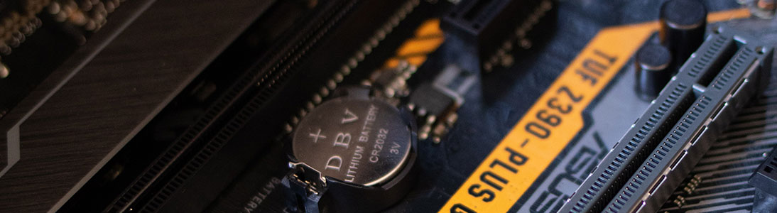
The activity of extra discounts on wholesale prices is in full swing…
Please fill in your contact information and we will send you the latest wholesale price list.